|
SIMPLE ELECTRONIC KEYER |
| BY N1HFX |
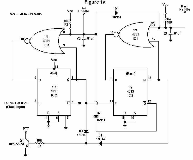
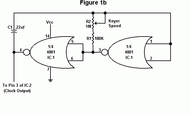
Serious CW operators know that a paddle is the way to go to make CW easy and fun. But along with the paddle, a certain amount of electronics is needed to produce the necessary dots and dashes. This circuit in figures 1a and 1b is a simple keyer which can be built for as little as $6 with some junk box parts. Although this circuit is not a true iambic keyer, it is capable of producing perfectly sounding CW. To make construction easy, all parts are available off the shelf at any Radio Shack store.
The circuit in figures 1a and 1b uses a quad NOR gate chip and a dual-D flip-flop chip. Two of the NOR gates are used as the clock generator and the frequency is determined by C1, R1 and R2 which sets the keying speed. This clock signal is fed into Pin 3 of IC 2 which is the dot flip flop. Nothing happens at this point until the dot paddle is grounded. When the dot paddle is depressed, Pin 1 of the flip flop changes states for as long as the dot paddle is depressed. When the dash paddle is grounded, this in turn causes the dot paddle to be grounded also through Diode D1. This starts the dash cycle which continues until Pin 13 of IC-2 changes state again. Diode D2 keeps the dot paddle low until the dash cycle finishes. Pins 1 and 13 of each flip-flop form the output to transistor Q1. Because Pin 1 is not always high during the dash cycle, Diodes D3 and D4 form an OR gate to keep Q1 turned on during a dash cycle.
This circuit has one anomaly which operators should be aware of. The dash paddle always has priority and attempts to squeeze the paddle (both dot and dash depressed) results in a continuous stream of dashes. This means the operator must release the dash paddle before depressing the dot paddle. Experienced CW operators will have no problem with this circuit but sloppy high speed operators will need to refine their sending since it is not as forgiving as a Curtis chip.
This circuit uses CMOS chips which require special handling to prevent static charges. IC sockets are highly recommended. The circuit requires very low power and can be powered from 8 to 15 volts. A 9 volt battery should last several months meaning an on/off switch isn't needed. No weight control is provided because experience has shown that it is often misused by operators causing code which is difficult to copy. A shielded enclosure is required and capacitors C2 and C3 should be soldered as close to the paddle jack as possible to keep RF out of the circuit. This circuit was constructed on a Radio Shack multipurpose pc board (RS 276-150) and no printed circuit board is available for this project.
DE N1HFX
Parts List
| R1 | 100K resistor, ¼ watt 5% tolerance (RS 271-1347) |
| R2 | 1 Meg potentiometer (RS 271-211) |
| R3,R4,R5 | 10K resistor, ¼ watt 5% tolerance (RS -271-1335) |
| C1 | .22 microfarad capacitor (RS 272-1070) |
| C2,C3 | .01 microfarad capacitor (RS 272-1065) |
| D1,D2,D3,D4 | 1N914/1N4148 or similar diode (RS 276-1122) |
| Q1 | 2N2222A or similar NPN general purpose transistor (RS 276-2009) |
| IC-1 | 4001 quad NOR gate (RS 276-2401) |
| IC-2 | 4013 dual D-type flip-flop (RS 276-2413) |

